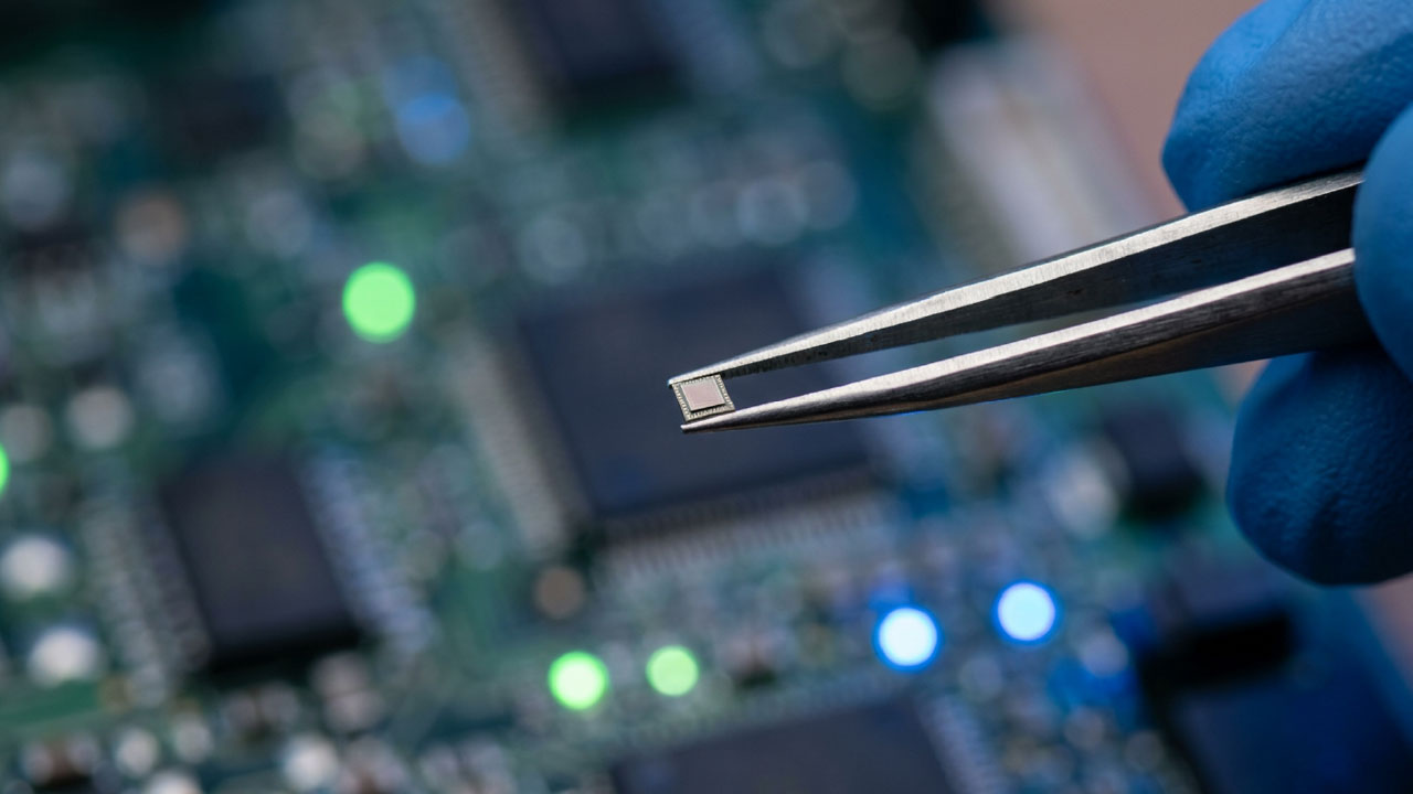
One of the biggest advances in the semiconductor market in recent decades was recently announced. IBM introduced the world's first sub-1 nanometer chip, an unprecedented architecture called Nanostack. With just 0,7 nanometer (or 7 angstroms), the novelty represents a new generation of processors aimed at artificial intelligence (IA), high performance computing and data centers.
For that, Nanostack reaches almost 100 billions of transistors on a chip the size of a fingernail, with twice the density of the chip 2 nanometers launched in 2021. With modular structure and adaptable to CPUs, GPUs, mobile chips and custom circuits, This would be a solution with greater efficiency and overall performance. When making this release, IBM reinforced its position among the main semiconductor research centers.
The novelty arrives four years after another milestone reached by IBM itself, which presented the 2 nanometers based on nanosheet architecture. As happened in the previous model, The company's expectation is that it will be widely used in the industry.
The technology difference
This chip represents an innovation in the semiconductor industry as it allows the stacking of transistors, increasing the number of components in the same space and increasing performance without having to increase the size of the product. This advance is important because semiconductors are the basis of virtually all modern electronic equipment., and its evolution drives areas such as AI, cloud computing and various digital systems.
“All of this is important because semiconductors are the basis of modern life, powering everything from artificial intelligence systems and cloud infrastructure to devices, critical networks and systems that society and businesses depend on daily”, explicou Jay Gambetta, director of IBM Research and IBM Fellow.
50% more performance
The tests carried out and published by the manufacturer point to an improvement of up to 50% on chip performance and 70% in energy efficiency, depending on the configuration adopted at the time of design. Regarding computing for AI, where energy costs already represent one of today’s main challenges, innovation predicts a reduction of up to 70% in consumption without giving up processing capacity.
Yet, initial tests indicate an improvement in 40% in scaling SRAM memory in relation to the chip 2 nanometers, unprecedented advance in recent 12 years, according to IBM.